

1. 流程介绍
PKE RSSI Single 配置流程(其中细节部分并没有全部展示)如 图 1.1 所示。
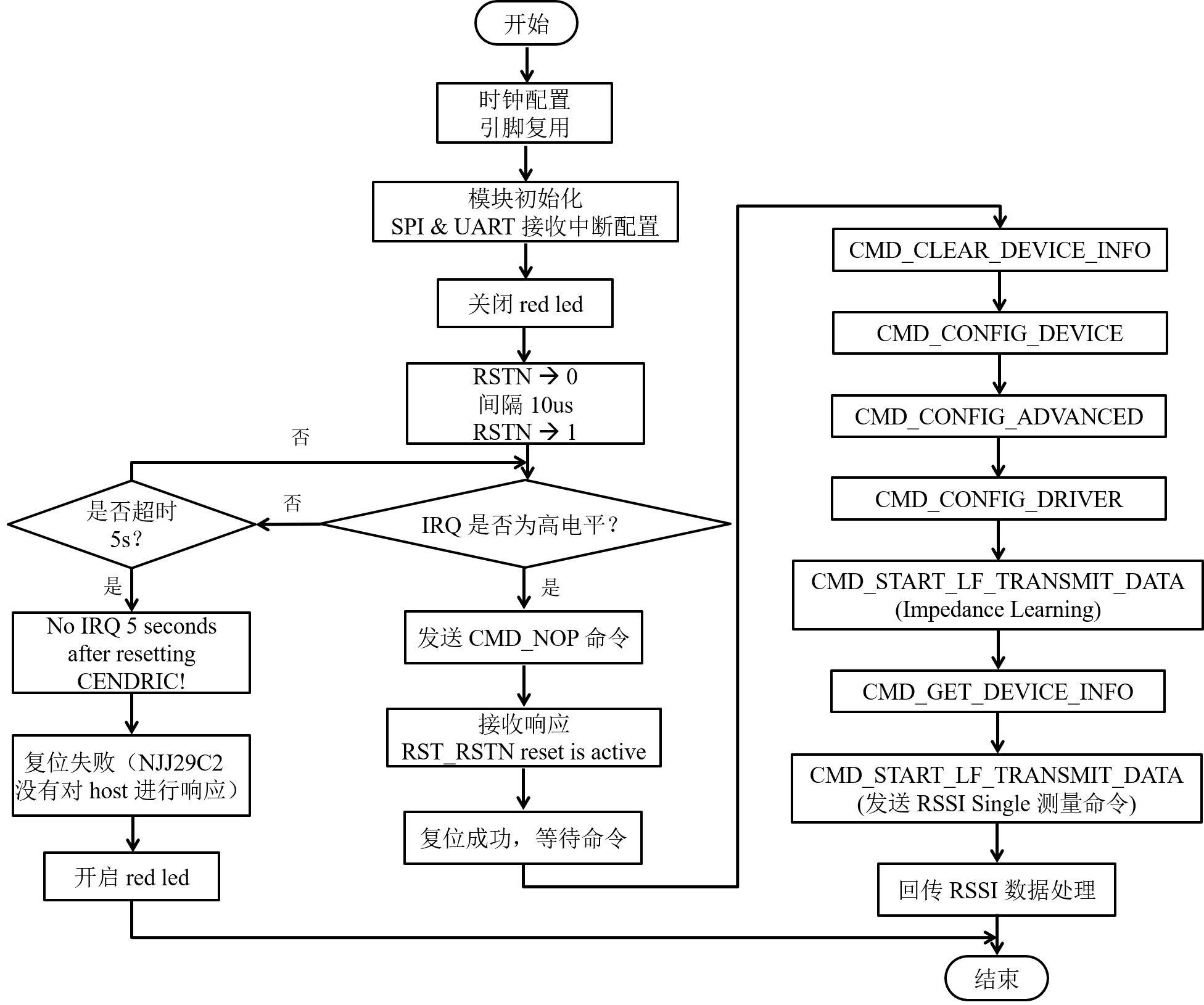
图 1.1 PKE RSSI Single 配置流程图
图 1.2 是 RSSI Single 时整体硬件环境搭建的截图,高频接收使用的是 NCK2912,基站板上 OLED 可以显示钥匙 NCF29A1 测试得到的 X、Y、Z 三轴的 RSSI 数据。
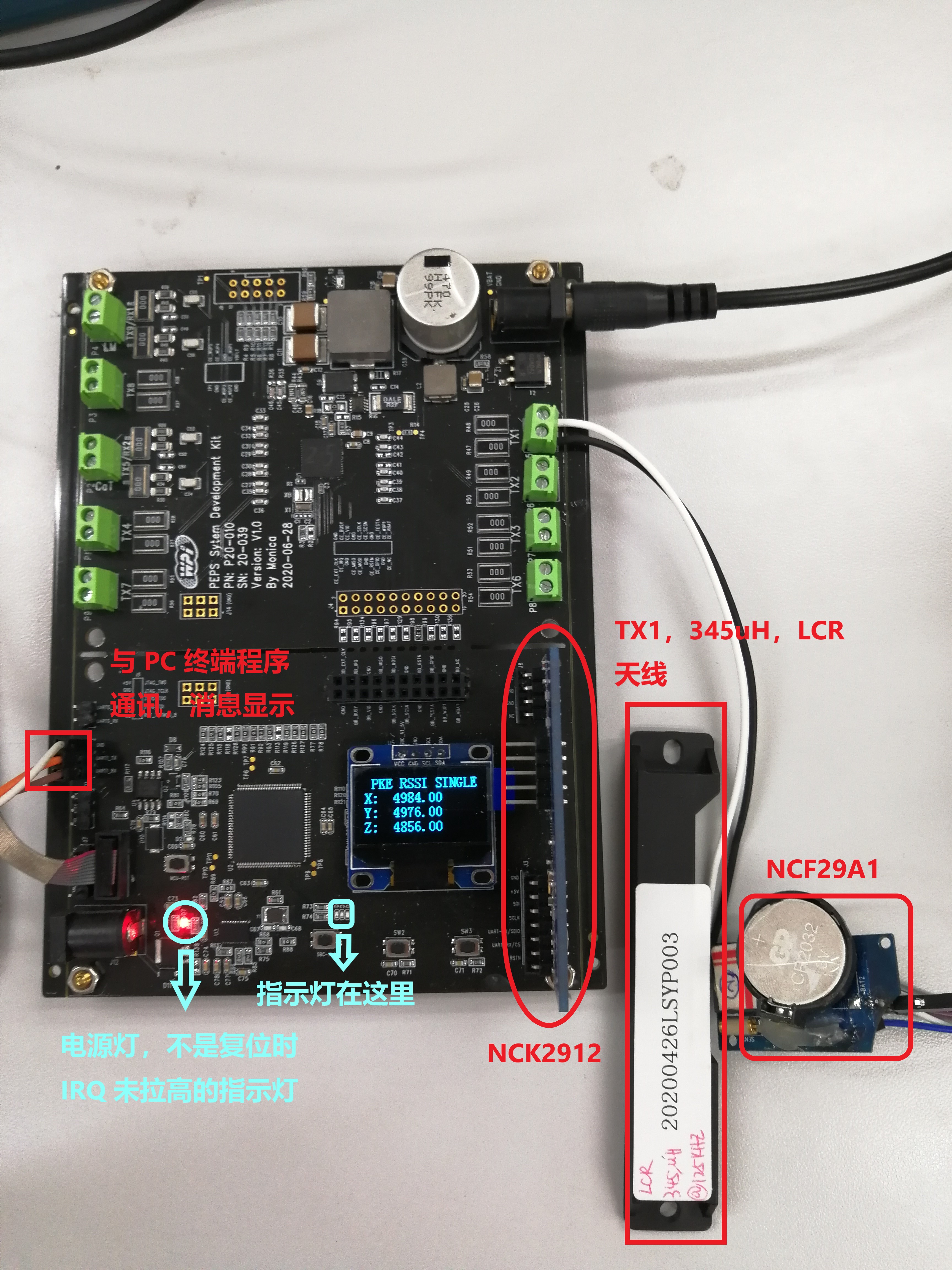
图 1.2 硬件环境搭建
图 1.3 是终端程序消息显示(波特率 115200),其中包含了整个过程中 S32K144 和 NJJ29C2 之间通信的数据帧,其中包含有所唤醒钥匙 ID(处理过的) 以及 RSSI 命令。
|
[15:59:48.008]收←◆ Running the S32K144_PKE_RSSI_SINGLE project. 2020.08.25 [15:59:48.338]收←◆ (CMD Frame): 00 00 00 00 00 00 00 00 00 00 00 00 00 00 00 00 00 00 00 00 00 00 00 00 00 00 00 00 00 00 2A 45 CENDRIC VERSION: ******************************* ***** Hardware Version: 3 ***** ***** Major Version: 3 ***** ***** Minor Version: 0 ***** ******************************* (RESP_GENERIC Frame): 20 C0 00 01 09 C0 18 00 00 00 00 00 00 00 00 00 00 00 00 00 00 00 00 00 00 00 1F 00 00 00 47 FD (CMD Frame): 8A 01 00 00 00 00 00 00 00 00 00 00 00 00 00 00 00 00 00 00 00 00 00 00 00 00 00 00 00 00 4F 61 (CMD Frame): 81 08 02 04 40 21 01 D5 FF 10 00 00 00 01 FF FF 00 00 00 00 00 00 00 00 00 00 00 00 00 00 4F FD (CMD Frame): 90 03 BB B3 E5 15 F2 00 00 00 00 00 00 00 00 00 00 00 00 00 00 00 00 00 00 00 00 00 00 00 B9 FD (CMD Frame): 02 ED 02 28 44 ED 28 F0 10 82 38 3F EB 30 F0 00 00 00 00 00 00 00 00 00 00 00 00 00 00 00 E0 E3 (CMD Frame): 00 00 00 00 00 00 00 00 00 00 00 00 00 00 00 00 00 00 00 00 00 00 00 00 00 00 00 00 00 00 2A 45 CENDRIC VERSION: ******************************* ***** Hardware Version: 3 ***** ***** Major Version: 3 ***** ***** Minor Version: 0 ***** ******************************* (RESP_GENERIC Frame): 20 00 00 00 09 C0 18 00 00 00 00 00 00 00 00 00 00 00 00 00 00 00 00 00 00 00 1F 00 00 00 10 5B (CMD Frame): 83 04 01 20 04 05 00 00 00 00 00 00 00 00 00 00 00 00 00 00 00 00 00 00 00 00 00 00 00 00 77 0E (CMD Frame): 00 00 00 00 00 00 00 00 00 00 00 00 00 00 00 00 00 00 00 00 00 00 00 00 00 00 00 00 00 00 2A 45 CENDRIC VERSION: ******************************* ***** Hardware Version: 3 ***** ***** Major Version: 3 ***** ***** Minor Version: 0 ***** ******************************* (RESP_GENERIC Frame): 20 00 04 00 09 C0 18 00 00 00 00 00 00 00 00 00 00 00 00 00 00 00 00 00 00 00 1B 01 00 00 7F CA (CMD Frame): 09 02 00 00 00 00 00 00 00 00 00 00 00 00 00 00 00 00 00 00 00 00 00 00 00 00 00 00 00 00 9A 4F (CMD Frame): 00 00 00 00 00 00 00 00 00 00 00 00 00 00 00 00 00 00 00 00 00 00 00 00 00 00 00 00 00 00 2A 45 ****************************************** ******* Impedance Learning Results ******* ****************************************** the min VDR: 14.6 V the max VDR: 14.6 V DR1_ZEFF: 11.25 Ohm DR1_PHASE: 34.30 degree DR1_CURRENT: 412.50 mA ****************************************** (RESP_DIAG Frame): 23 49 49 2D 31 42 54 00 00 28 00 00 28 00 00 38 00 00 28 00 00 28 00 00 28 00 00 38 00 00 F9 9D [15:59:48.370]收←◆ (CMD Frame): 03 0B 01 20 00 37 A6 6F 35 1F 02 50 9D 04 01 20 02 5D 00 00 00 00 00 00 00 00 00 00 00 00 A5 33 [15:59:48.519]收←◆ RSSI(NXP) X: 4984.00 RSSI(NXP) Y: 4976.00 RSSI(NXP) Z: 4856.00 |
图 1.3 终端程序 SPI 消息帧显示
1. 引脚复用
因为时钟配置在之前 S32K144 Clock Module 中已经介绍过了,这里就不在赘述,只是需要介绍一下,PEPS 方案中所使用到的引脚的复用情况。其中需要注意的是,与 NJJ29C2 RSTN、BUSY 以及 IRQ 相连的引脚是配置成 GPIO,以便执行 NJJ29C2 复位,检查 NJJ29C2 是否正忙(此时需要等待,不能再发 SPI 命令),检查 NJJ29C2 是否有响应。
具体代码如下:
|
void Port_Init(void) { /* PORT clock enable */ ENABLE_PORT_CLOCK(PCC_PORTA_INDEX); ENABLE_PORT_CLOCK(PCC_PORTB_INDEX); ENABLE_PORT_CLOCK(PCC_PORTC_INDEX); ENABLE_PORT_CLOCK(PCC_PORTD_INDEX);
/* PTC16 is used as GPIO: Simulated IIC SDA */ CFG_PIN_FUNCTION(PORTC, PTC16, Alt1);
/* PTC17 is used as GPIO: Simulated IIC SCL */ CFG_PIN_FUNCTION(PORTC, PTC17, Alt1);
/* GPIO: RGB LED */ CFG_PIN_FUNCTION(PORTD, PTD15, Alt1); /* RED LED */ CFG_PIN_FUNCTION(PORTD, PTD16, Alt1); /* GREEN LED */ CFG_PIN_FUNCTION(PORTD, PTD0, Alt1); /* BLUE LED */
/* Control & Indicator: * PTB11 --> RSTN * PTC10 --> BUSY * PTC11 --> IRQ */ CFG_PIN_FUNCTION(PORTB, PTB11, Alt1);
CFG_PIN_FUNCTION(PORTC, PTC10, Alt1); Port_Internal_Pull_Down(PORTC, PTC10); /* enable pull-down resistor if input configured */
CFG_PIN_FUNCTION(PORTC, PTC11, Alt1); Port_Internal_Pull_Down(PORTC, PTC11); /* enable pull-down resistor if input configured */
/* For Debug: * PTB1 --> LPUART0_TX * PTA2 --> LPUART0_RX */ CFG_PIN_FUNCTION(PORTB, PTB1, Alt2); CFG_PIN_FUNCTION(PORTA, PTA2, Alt6);
/* Connect to PC: * PTC7 --> LPUART1_TX * PTC6 --> LPUART1_RX */ CFG_PIN_FUNCTION(PORTC, PTC7, Alt2); CFG_PIN_FUNCTION(PORTC, PTC6, Alt2);
/* Connect to RF Receiver: * PTD7 --> LPUART2_TX * PTD6 --> LPUART2_RX */ CFG_PIN_FUNCTION(PORTD, PTD7, Alt2); CFG_PIN_FUNCTION(PORTD, PTD6, Alt2);
/* PTB0 is used as LPSPI1_PCS0 * PTB2 is used as LPSPI1_SCK * PTB3 is used as LPSPI1_SIN * PTB4 is used as LPSPI1_SOUT */ CFG_PIN_FUNCTION(PORTB, PTB0, Alt3); CFG_PIN_FUNCTION(PORTB, PTB2, Alt3); CFG_PIN_FUNCTION(PORTB, PTB3, Alt3); CFG_PIN_FUNCTION(PORTB, PTB4, Alt3);
} |
LPUART 接收中断使能,在之前的文档 S32K144 LPUART Module 已经有介绍,就不再说明。
这里只是要介绍一下,由于 SPI 数据的传送(双向,S32K144 à NJJ29C2 以及 S32K144 ß NJJ29C2)是同时发生,如果是按照最基本的方式(发送完数据后再去接收),是无法接收到响应数据的。所以 NXP 推荐了两种方式:一种是中断,另一种则是 DMA。
本篇文章只介绍 LPSPI 中断接收的配置,因为这已经能够实现 S32K144 以及 NJJ29C2 的正常通讯。
另外 NXP 也强调过,在一个完整的命令(32 bytes)收发期间,SCSN 必须保持低电平。因为它的上升沿已经被定义为帧的结束,之后 NJJ29C2 会开始处理。所以如果不能保证 SCSN 在这期间为低电平的话,可能会造成回传的响应时钟重复 Response code(如 0x20)。如果一个数据帧结束之后,如果实际传输的字节数与预期的字节数不一致,也会导致传输数据被丢弃,IRQ 也会变为高电平来通报故障。
关于 LPSPI 初始化的配置代码及说明请参考 附录 1,以下是关于 LPSPI 接收中断的配置代码:
|
LPSPI.h |
|
typedef void (*LPSPI_CallbackType) (LPSPI_MemMapPtr pLPSPI); |
|
LPSPI.c |
|
LPSPI_CallbackType LPSPI_Callback = NULL; …… void LPSPI_SetCallback(LPSPI_CallbackType pfnCallback) { LPSPI_Callback = pfnCallback; }
void LPSPI0_IRQHandler (void) { LPSPI_Callback (LPSPI0); } |
|
rssiSingle_Main.c |
|
void LPSPI0_ISR(LPSPI_MemMapPtr pLPSPI) { /* read received data */ cendricRespData[cendricRespIndex] = LPSPI0->RDR; cendricRespIndex++;
/* the index should not exceed 32 bytes */ cendricRespIndex &= 0x1F; } …… /* LPSPI0 Module Initialization */ LPSPI0_Init_Master();
/* Enable LPSPI0 interrupt */ S32K144_Enable_Interrupt(LPSPI0_IRQn); S32K144_NVIC_SetNonCorePriority(LPSPI0_IRQn, 6); /* priority 6 of 0-15 */
/* set up callback routine */ LPSPI_SetCallback(LPSPI0_ISR); |
S32K144 通过 PTB11 控制 NJJ29C2 RSTN 复位,然后便会在 5s 的时间范围内检测是否 IRQ 置高,因为当前 NJJ29C2 处于 ERROR 状态,NJJ29C2 会通过 RESP_GENERIC 向 S32K144 汇报该信息。一旦检测到 IRQ 置高,S32K144 就会发送 CMD_NOP 命令,取回 RESP_GENERIC。之后要想 NJJ29C2 能够正常处理 S32K144 发送的 SPI 命令,需要保证 NJJ29C2 从 ERROR 状态退出回到 IDLE 状态,这个时候就需要发送 CMD_CLEAR_DEVICE_INFO 将对应的复位信息清理掉。
具体代码如下所示:
|
uint8_t rstnPin_Cendric_Reset (void) { uint16_t timeCount_5s = 0;
/* pull down the level of RSTN pin of CENDRIC for 1ms to reset */ OUTPUT_CLEAR(PTB, PTB11); Delay_ms(1); OUTPUT_SET(PTB, PTB11);
for ( ; ; ) { /* check the IRQ line in cycle in 5s*/ if(is_pit_triggered()) { ++timeCount_5s;
if(5000 <= timeCount_5s) { printf("\nNo IRQ 5s after resetting CENDRIC..."); return Cendric_NoIrq; }
if(is_Irq_HighLevel()) {
Cendric_CMD_NOP(0);
Cenric_RESP(cendricRespData, CENDRIC_SPI_LENGTH);
/* clear reset source after reset */ Cendric_CMD_CLEAR_DEVICE_INFO(1, cendricClrRstnRst , sizeof(cendricClrRstnRst));
/* restore counter, reset is done */ timeCount_5s = 0; return Cendirc_RstSuccess; }
} } |
4. NJJ29C2 基础配置 & Impedance Learning
该部分与文档《S32K144 CADS 调试》所描述的流程一致,参数设置上也没有太大区别,具体代码如下所示:
|
* Note: the length is not fixed,which can be changed */ uint8_t cendricConfigDev[15] = { 0x08, 0x02, 0x04, 0x40, 0x21, 0x01, 0xD5, 0xFF, 0x10, 0x00, 0x00, 0x00, 0x01, 0xFF, 0xFF }; uint8_t cendricConfigAdvanced[6] = { 0x03, 0xBB, 0xB3, 0xE5, 0x15, 0xF2 }; uint8_t cendricConfigDrv[14] = { 0xED, 0x02, 0x28, 0x44, 0xED, 0x28, 0xF0, 0x10, 0x82, 0x38, 0x3F, 0xEB, 0x30, 0xF0 }; uint8_t cendricImpLearning[5] = { 0x04, 0x01, 0x20, 0x04, 0x05 }; uint8_t cendricDiagResp[1] = { 0x02 }; uint8_t cendricClrRstnRst[1] = { 0x01 }; …… /* starts PKE LF frame transmission at tx1(High Power Mode) with 1Ap */ /* HPDR mode TX1-TX2 */ Cendric_CMD_CONFIG_DEVICE(1, cendricConfigDev, sizeof(cendricConfigDev));
/* This will bring the LF driver duty cycle closer to the target value of 40% */ Cendric_CMD_CONFIG_ADVANCED(1, cendricConfigAdvanced, sizeof(cendricConfigAdvanced));
/* set initial ZEFF = 10 Ohm, initial inductance value = 345uH */ Cendric_CMD_CONFIG_DRIVER(0, cendricConfigDrv, sizeof(cendricConfigDrv));
Cendric_CMD_NOP(0);
Cenric_RESP(cendricRespData, CENDRIC_SPI_LENGTH);
/* Antenna TX1 impedance learning (384us CW without regulation) */ Cendric_CMD_START_LF_TRANSMIT_DATA(1, cendricImpLearning, sizeof(cendricImpLearning));
/* Wait for IRQ in 50ms */ if( timeout == wait_Irq(50)) { return pkeTask_False; }
Cendric_CMD_NOP(0);
Cenric_RESP(cendricRespData, CENDRIC_SPI_LENGTH);
/* get diagnostics information */ Cendric_CMD_GET_DEVICE_INFO(0, cendricDiagResp, sizeof(cendricDiagResp));
Cendric_CMD_NOP(0);
Cenric_RESP(cendricRespData, CENDRIC_SPI_LENGTH);
/* Wait at minimum 20ms between learning and 1st LF telegram */ Delay_ms(20); |
5. RSSI Single 测试命令低频信号发送
对于 RSSI 回传数据的处理并不是本篇的重点,所以就不再介绍,具体代码如下:
|
/* global char variable - IDE,change it according to Key Fob */ uint8_t gcv_Ide[4]={0xA6, 0x6F, 0x35, 0xE1}; …… uint8_t cendricRssiData[17] = { 0x0B,0x01,0x20,0x00,0x37,0x00,0x00,0x00,0x00, 0x02,0x50,0x9D,0x04,0x01,0x20,0x02,0x5D }; …… /* transmit RSSI Single Command via LF signal */ /* Wake Up ID transmitted */ /* 1. Swap last byte of IDE 2. OR with 0x0F */ gcv_Ide[3] = (gcv_Ide[3] & 0x00) | ((gcv_Ide[3] & 0x0F) << 4); gcv_Ide[3] |= 0x0F;
#if (DEBUG == 1) printf("\nWakeup ID Value:"); printf("%02X", giv_Wup); #endif
/* store giv_Wup in array to meet the requirements of SPI transmission sequence */ cendricRssiData[5] = gcv_Ide[0]; cendricRssiData[6] = gcv_Ide[1]; cendricRssiData[7] = gcv_Ide[2]; cendricRssiData[8] = gcv_Ide[3]; Cendric_CMD_START_LF_TRANSMIT_DATA(0, cendricRssiData, sizeof(cendricRssiData));
/* Wait for IRQ in 50ms */ if( timeout == wait_Irq(50)) { return pkeTask_False; } |
三、 参考资料
- Um525831 – NJJ29C2 Objective User Manual (Rev. 3.1, 19 June 2020)
- UM – SCA1903 – NJJ29C2 Customer Demo Operation (Rev. 3.0, 8 May 2020)
- NJJ29C2 Explanations about initializations of application examples (Rev. 1.0, 15 July 2020)
四、 附录
通过将 LPSPI TCR 寄存器的 CONT 写 1,可以保证 SCSN 在命令传输过程中保持低电平(连续传输),在发送结束后再次对 TCR 进行写入,可以使 SCSN 重新拉高。注意,TCR 寄存器需要将 32-bit 数据一次性写入。具体 LPSPI 初始化代码如下:
|
LPSPI.c |
|
void LPSPI0_Init_Master(void) { /* disable the LPSPI0 clock(clear first,then set parameters such as PCS etc) */ DISABLE_PORT_CLOCK(PCC_LPSPI0_INDEX);
/* PCC LPSPI0 Register configuration: * Field Descriptions * [31] PR 1b - Peripheral is present. * [30] CGC 1b - Clock enabled.Lock the clock selection.(can't change) * [26:24] PCS 110b - clock option 6(SPLLDIV2_CLK:40MHz) */ PCC->PCCn[PCC_LPSPI0_INDEX] |= PCC_PCCn_PR(0b1) | PCC_PCCn_CGC(0b1) | PCC_PCCn_PCS(0b110);
/* Disable LPSPI0 Module Configuration: * Field Descriptions * [9] RRF 0b - Receive FIFO not reset * [8] RTF 0b - Transmit FIFO not reset * [3] DBGEN 0b - LPSPI module is disabled in debug mode * [2] DOZEN 0b - LPSPI module is enabled in Doze mode * [1] RST 0b - Module is not reset * [0] MEN 0b - Module is disabled */ LPSPI0->CR = 0x00000000;
/* Interrupt : * Field Descriptions * [1] RDIE 1b - Receive Data Interrupt Enable * */ LPSPI0->IER |= LPSPI_IER_RDIE_MASK;
/* DMA request is disabled */ LPSPI0->DER = 0x00000000;
/* Configuration Register 0 setup: * Field Descriptions * [9] RDMO 0b - Received data is stored in the receive FIFO as in normal operations * [8] CIRFIFO 0b - Circular FIFO is disabled * [0] HREN 0b - Host request is disabled * */ LPSPI0->CFGR0 = 0x00000000;
/* Configuration Register 1 setup: * Field Descriptions * [27] PCSCFG 0b - PCS[3:2] are enabled * [26] OUTCFG 0b - Output data retains last value(not tri-state) when CS is negated * [25:24] PINCFG 00b - SIN is used for input data and SOUT is used for output data * [18:16] MATCFG 000b - Match is disabled * [11:8] PCSPOL 0000b - PCSx is active low * [3] NOSTALL 1b - Transfers will not stall when the transmit FIFO is empty or the receive FIFO is full * [2] AUTOPCS 0b - Automatic PCS generation is disabled * [1] SAMPLE 0b - Input data is sampled on SCK edge * [0] MASTER 1b - Master Mode */ LPSPI0->CFGR1 |= LPSPI_CFGR1_NOSTALL(0b1) | LPSPI_CFGR1_MASTER(0b1);
/* Transmit Command Register Configuration(only be written using 32-bit writes): * Field Description * [31] CPOL 0b - The inactive state value of SCK is low * [30] CPHA 1b - Data is changed on the leading edge of SCK and captured on the following edge of SCK * [29:27] Prescale 010b - Functional clock devided by 2^2 = 4 * [25:24] PCS 00b - Transfer using LPSPI_PCS[0] * [23] LSBF 0b - MSB first * [22] BYSW 0b - Byte Swap is disabled * [21] CONT 0b - Continuous transfer is enabled * [20] CONTC 0b - Command word for start of new transfer * [19] RXMSK 0b - Normal transfer * [18] TXMSK 0b - Normal transfer * [17:16] WIDTH 00b - 1-bit transfer * [11:0] FRAMESZ 000000000111b - the frame size equals to 7+1 = 8 bits */ LPSPI0->TCR = (LPSPI_TCR_CPOL(0b0) | LPSPI_TCR_CPHA(0b1) | LPSPI_TCR_PRESCALE(0b010) | LPSPI_TCR_PCS(0b00) | LPSPI_TCR_LSBF(0b0) | LPSPI_TCR_BYSW(0b0) | LPSPI_TCR_CONT(0b1) | LPSPI_TCR_CONTC(0b0) | LPSPI_TCR_RXMSK(0b0) | LPSPI_TCR_TXMSK(0b0) | LPSPI_TCR_WIDTH(0b00) | LPSPI_TCR_FRAMESZ(7));
/* Clock Configuration register setup(SPLLDIV2_CLK/PRESCALE = 40MHz/4 = 10MHz <=> 100ns): * Field Description * [31:24] SCKPCS 0x04 - SCK-to-PCS delay equals to (4+1 = 5)cycles of functional clock divided by TCR[PRESCALE] * [23:16] PCSSCK 0x09 - PCS-to-SCK delay equals to (9+1 = 10)cycles of functional clock divided by TCR[PRESCALE] * [15:8] DBT 0x1C - delay between transfers is (28+2 = 30)cycles of functional clock divided by TCR[PRESCALE] * [7:0] SCKDIV 0x08 - SCK period equals to (8+2 = 10)cycles of functional clock divided by TCR[PRESCALE] */ LPSPI0->CCR |= LPSPI_CCR_SCKPCS(0xFF) | LPSPI_CCR_PCSSCK(0xFF) | LPSPI_CCR_DBT(28) | LPSPI_CCR_SCKDIV(8);
/* FIFO Control Register Configuration: * Field Description * [17:16] RXWATER 00b - RX Flag is set when the number of words in RX FIFO > 0 * [1:0] TXWATER 03b - TX Flag is set when the number of words in TX FIFO <= 0 */ LPSPI0->FCR |= LPSPI_FCR_RXWATER(0b00) | LPSPI_FCR_TXWATER(0b00);
/* Enable LPSPI0 Module Configuration: * Field Descriptions * [9] RRF 0b - Receive FIFO not reset * [8] RTF 0b - Transmit FIFO not reset * [3] DBGEN 1b - LPSPI module is disabled in debug mode * [2] DOZEN 0b - LPSPI module is enabled in Doze mode * [1] RST 0b - Module is not reset * [0] MEN 0b - Module is disabled */ LPSPI0->CR |= LPSPI_CR_DBGEN(0b1) | LPSPI_CR_MEN(0b1);
} …… /* The host shall not send any further SPI frame to NJJ29C2 * when the BUSY line is high, as it will not be stored and the data is lost. */ bool is_Busy_HighLevel( void ) { bool tmp; tmp = (bool)((PTC->PDIR >> PTC10) & 1);
return tmp; }
uint8_t LPSPI0_Transmit_8bits(uint8_t *send, uint8_t txLength) { uint8_t i; bool isHighLevel;
/* the length should not be zero */ if (0 == txLength) { return spiCom_False; }
if (true == is_Busy_HighLevel()) { do { isHighLevel = is_Busy_HighLevel(); if (timeout == is_timeout(5000)) {
printf("\nCMD can not be send,because BUSY Line maintains high for 5s...");
return spiCom_False; } } while(isHighLevel == is_Busy_HighLevel()); }
for(i = 0; i < txLength; i++) {
/* wait for TX FIFO available */ while(!(LPSPI0->SR & LPSPI_SR_TDF_MASK));
/* transmit data */ LPSPI0->TDR = send[i];
if((i % 4) == 0) { LPSPI0_Set_TxDelay(0xC6); /* delay 20us between transfers */ } else { LPSPI0_Set_TxDelay(0x1C); /* delay 3us between transfers */ }
}
/* write an extra Transmit Command word to negative the SCSN */ LPSPI0->TCR = (LPSPI_TCR_CPOL(0b0) | LPSPI_TCR_CPHA(0b1) | LPSPI_TCR_PRESCALE(0b010) | LPSPI_TCR_PCS(0b00) | LPSPI_TCR_LSBF(0b0) | LPSPI_TCR_BYSW(0b0) | LPSPI_TCR_CONT(0b1) | LPSPI_TCR_CONTC(0b0) | LPSPI_TCR_RXMSK(0b0) | LPSPI_TCR_TXMSK(0b0) | LPSPI_TCR_WIDTH(0b00) | LPSPI_TCR_FRAMESZ(7));//0x53000007;
return spiCom_Success; } |
评论