

介绍
标准定义了一个可扩展的数字显示接口,具有可选的音频和内容保护功能,可广泛应用于PC和消费电子(CE)设备。该接口设计支持
1.内部芯片到芯片
2.外部盒到盒的数字显示连接。
潜在的内部芯片到芯片的应用包括在笔记本电脑中使用图形控制器驱动面板,以及在显示器或电视中使用显示控制器驱动显示组件。
用于显示端口的盒对盒应用程序示例包括pc与监视器、投影仪和电视显示器之间的显示连接。
DisplayPort也适用于消费类电子设备之间的显示连接,如高清光盘播放器、机顶盒和电视显示器。
Table 1-1: List of Acronyms Acronym Stands
- ACT Allocation Change Trigger
- API Application Programming Interface.
- AUX Auxiliary
- BER Bit Error Rate
- bpc Bits Per Component
- bpp Bits Per Pixel
- BE Blanking End
- BS Blanking Start
- CDR Clock and Data Recovery
- CEA Consumer Electronics Association
- CP Content Protection
- CVT Coordinated Video Timings (VESA)
- DB Data Byte
- DDC/CI Display Data Channel/Command Interface (VESA)
- DPCP DisplayPort Content Protection
- DPCD DisplayPort Configuration Data
- DJ Deterministic Jitter
- DMT Discrete Monitor Timing (VESA)
- DP DisplayPort (VESA)
- DPCD DisplayPort Configuration Data
- DP_PWR DP Power
- eDP Embedded DisplayPort (VESA)
- ECC Error Correcting Code
- ECF Encryption Control Field
- E-DDC Enhanced Display Data Channel (VESA)
- EDID Extended Display Identification Data (VESA)
- EOS Electrical Over-Stress
- EMT End of Message Transaction
- ESD Electro Static Discharge
- FAUX Fast AUX
- GPU Graphics Processor Unit
- GUID Globally Unique ID
- HB Header Byte
- HBR High Bit Rate (2.7Gbps per lane)
- HBR2 High Bit Rate 2 (5.4Gbps per lane)
- HDCP High-bandwidth Digital Content Protection
- HPD Hot Plug Detect
- I2C Inter-IC
- IRQ Interrupt Request
- ISI Inter-Symbol Interference
- LFSR Linear Feedback Shift Register.
- lsb Least Significant Bit
- LPCM Linear Pulse Code Modulation
- LVP Link Verification Pattern
- Maud M value for audio
- MCCS Monitor Control Command Set (VESA)
- msb Most Significant Bit
- MOT Middle Of Transaction
- MST Multi-Stream Transport
- MTP Multi-stream Transport Packet
- MTPH Multi-stream Transport Packet Header
- Mvid M value for video
- Naud N value for audio
- nb Nibble
- Nvid N value for video
- NORP Number Of Receiver Ports
- OCP Over Current Protection
- OUI Organizational Unique ID
- PB Parity Byte
- PCB Printed Circuit Board
- PRBS Pseudo Random Bit Sequence
- RBR Reduced Bit Rate
- RG Rate Governing
- RGB Red Green Blue
- RJ Random Jitter
- RTL Register Transfer Level
- RX Receiver
- SDP Secondary-Data Packet
- SE SDP End
- SF Stream Fill
- SR Scrambler Reset
- SS SDP Start
- SSC Spread Spectrum Clock
- SST Single-Stream Transport
- TCON Timing Controller
- TDR Time Domain Reflectometry
- TIA Timing Interval Analyzer
- TIE Timing Interval Error
- TJ Total Jitter
- TU Transfer Unit
- TX Transmitter
- UI Unit Interval
- VB-ID Vertical Blanking ID
- VESA Video Electronics Standards Association
- VHDL Very high speed integrated circuit Hardware Description Language
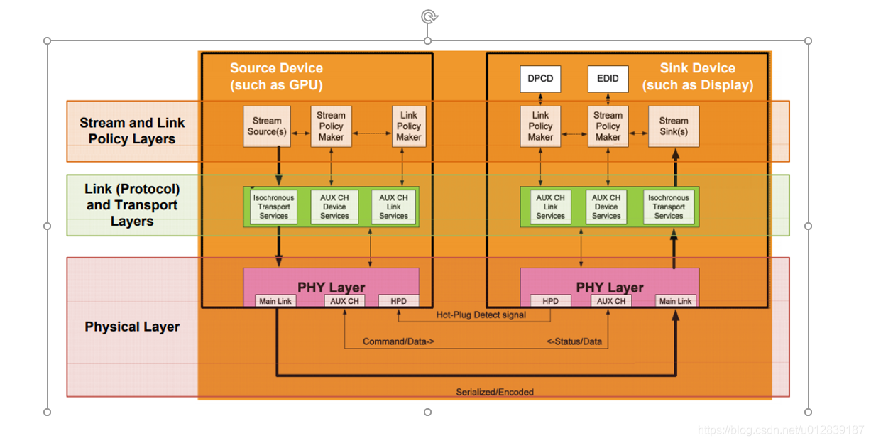
链路层
介绍配置和管理协议,数据的传输[host->display]转发传输通道以及辅助双向通道,包括SST[single steam transport]以及MST[multi-stream transport]。
物理层
物理层部分描述了显示端口发射机和接收机实现的电气要求。它还定义了所需的电路和编码方法,用于通过电缆或线路板跟踪在显示端口链路层之间来回传输数据DPCP对应的是link policy marker,描述的是接收方的能力;EDID对应的是stream policy marker,描述的是接收设备。
link/stream policy marker分别管理对应的link和stream;流策略制定者管理流的传输。链接策略制定者管理链接并负责保持链接同步。
Displayport 组件
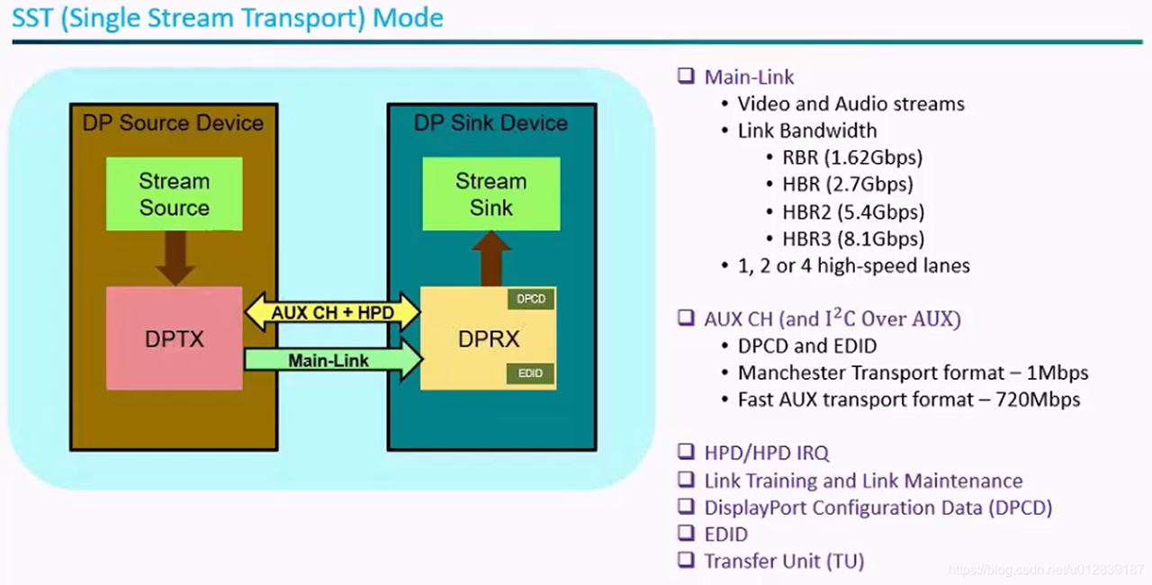
Displayport link,连接source和sink的通路,包含:Main link[不同的位宽,最多4lane,主要数据包传输] + Aux Channel[访问DPCD与EDID的专用链路] + HPD channel[hot-plug检测]
Main link用于传输视频和音频的数据路,main link由多个同时运行的单向串行数据通道组成,一般来说,最多由4条数据通道组成。在标准DisplayPort连接中,每个通道都有一组专用的双绞线,并使用差分信号在整个通道上传输数据。这是一个自计时系统,因此不需要专用的时钟信号通道。当建立连接时,DisplayPort Mainlink使用的传输模式由Source设备和Sink设备通过称为Link training的过程进行协商。此过程确定连接的最大可能速度。例如,如果DisplayPort电缆的质量不足以可靠地处理HBR2速度,则DisplayPort设备将检测到该情况并切换到较低的模式以保持稳定的连接。[听起来和usb的连接方式有点像];在视频消隐间隔(视频数据的每一行和每一帧之间短暂的停顿)期间,音频数据通过主链路传输。
AUX(Auxiliary)的用途包括读取扩展显示识别数据(EDID),以确保DP信号的正确传输;读取显示器所支持的DP接口的信息,如主要通道的数量和DP信号的传输速率;进行各种显示组态暂存器的设定;读取显示器状态暂存器。DisplayPort AUX通道是半双工双向数据通道,用于由设备制造商自行决定是否使用视频和音频以外的其他附加数据(例如I2C或CEC命令)。
数据位宽计算
A resolution can be supported only if the pixel stream BW is less than or equal to link symbol BW
Pixel stream BW = pixel clock * bpp / 8
Link symbol BW = link symbol clock * number of lanes
4K@30fps with 24bpp is supported by 2.7Gbps link @ 4 lanes but 30bpp requires 5.4Gbps link @ 4 lanes
Pixel clock for 4K@30fps is 297MHz
At 24bpp color depth, the pixel stream BW is 297*24/8 = 891 MBps
At 30bpp color depth, the pixel stream BW is 297*30/8 = 1113.75 MBps
For a 2.7Gbps link with 4lanes,
Link symbol clock = link rate * efficiency = 2700Mbps * 0.8
Converting to MBps, link symbol clock is 270MBps
Link symbol BW is 270 * 4 (lanes) = 1080 MBps
Similarly, link symbol BW for a 5.4Gbps lane with 4 lanes is 2160 MBps
MST vs SST
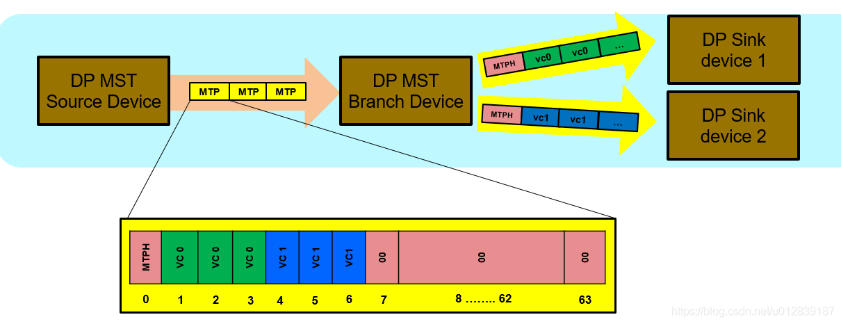
通过将多个视频流多路复用为一个流并将其发送到分支设备,该设备可以从源设备上的单个DP端口驱动多个独立的显示器,然后将其解复用为原始流。分支设备通常以MST集线器的形式出现,该MST集线器插入单个DP输入端口并提供多个输出,但也可以在显示器上内部实现,以提供用于Daisy-chaining的DP输出端口,从而有效地嵌入显示屏内部的2端口MST集线器。
aux通道和hpd线构成了MST链路管理的边带通道边带消息是用来检测拓扑的设备由GUID和相对地址唯一标识GUID帮助识别拓扑中的并行路径和循环,并采取纠正措施目的和元数据在边带消息头中编程。
评论