

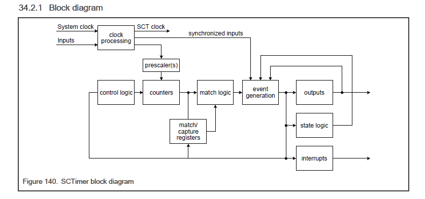
1. SCTIMER 定时器介绍
LPC5536 是基于 Arm®Cortex®-M33 处理器开发的 32 位微控制器, 它同时具备了高性能和低功耗的特点。其外设集成了两个高级定时器,即 eFlexPWM0 和 eFlexPWM1,可以用于控制两个 PMSM 电机,如果要控制多于 2 个电机,则需要使用 SCTIMER 来生成 PWM,SCTIMER 有一个 32 位或者可分成 2 个 16 位的 COUNTER 计时器,SCTIMER 由事件和状态驱动,事件的产生可以是计时器计时到 MATCH 值时,或者是输入、输出引脚产生上升沿或下降沿时,事件产生后可以切换状态,这些操作都是由硬件完成,不需要软件参与,其框图如下图所示:
本文例程主要讲述如何配置 SCTIMER 定时器生成 8 路 PWM,用于控制两个步进电机,下图红框部分,另两个步进电机使用 eFlexPWM0 控制,框图为: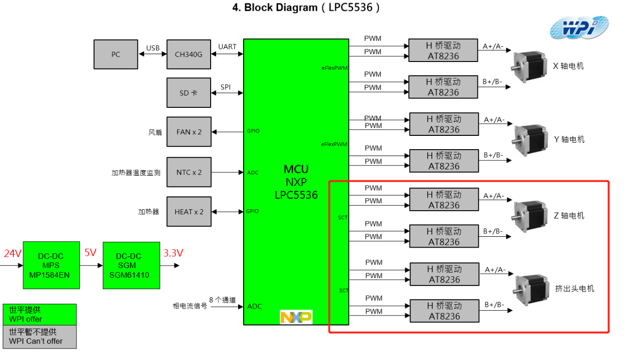
2. PWM 生成示意图
使用 MATCH0 配置 PWM 周期,同时设置计时器计数模式为 count up and count down 模式, 则 match0 计算方式为:sctimer clock/pwm/2 = 150000000/20000/2 = 3750,使用其他 MATCH 寄存器设置 PWM 产生上升沿的时刻,从而实现调整占空比的目的,通过将事件 EVENT 关联到此 MATCH,计时器计到此 MATCH 时产生此 EVENT,此事件使 SCTIMER 的输出引脚设置为高电平,输出引脚同时设置为自动翻转电平模式,实现中心对齐的 PWM,如下示意图所示: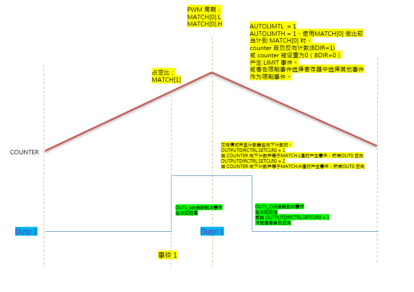
3. 配置和初始化 SCTIMER
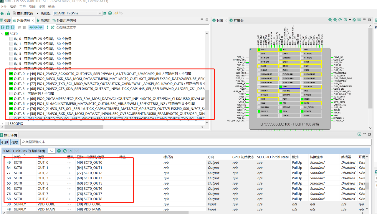
使用 MCUXpresso Config Tools 可以方便的配置 SCTIMER 的时钟和引脚配置,并自动生成 C 代码,在 main 函数中调用即可,分别如下图所示:蓝色为 SCTIMER 时钟路径,红框为 GPIO 输出引脚配置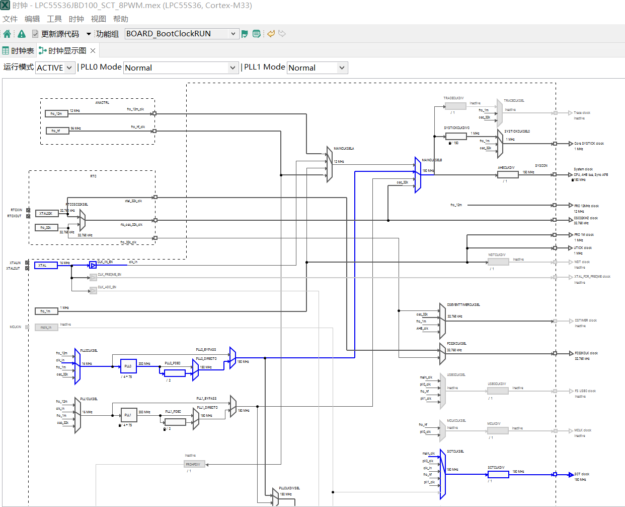
4. 初始化代码
如下为初始化代码,其每一位都做了详细备注,可结合 RM 查看。
/*
clock: 150MHz main_clock
Center Aligned
counter counts up to its limit, then counts down to 0.

*/
void SCT0_PWM_Init(void)
{
  /* Enable the SCTimer clock*/
  SYSCON->AHBCLKCTRLSET[1] = (1UL << 2UL);

  /* Reset the module. */
  SYSCON->PRESETCTRLSET[1] = (1UL << 2UL);
  while(0U == (SYSCON->PRESETCTRL1 & 0x4))
  {
    /* */
  }
  SYSCON->PRESETCTRLCLR[1] = (1UL << 2UL);
  while(0x4 == (SYSCON->PRESETCTRL1 & 0x4))
  {
    /* */
  }

  /* SCT CLK Configure */
  SYSCON->SCTCLKSEL = (SYSCON->SCTCLKSEL & 0xFFFFFFF8);//main_clock

  SCT0->CONFIG |= (1 << 0)|  /* UNIFY = 1 */
                  (0 << 1)|  /*
                              PWM clock mode:
                              0x0 System Clock Mode
                              0x1 Sampled System Clock Mode
                              0x2 SCT Input Clock Mode
                              0x3 Asynchronous Mode
                              */
                  (8 << 3)|  /* CKSEL */
                  (0 << 7)|  /* NORELAOD_L */
                  (0 << 8)|  /* NORELAOD_H */
                  (0 << 9)|  /* INSYNC:Synchronization for input N */
                  (1 << 17)| /* AUTOLIMIT_L */
                  (1 << 18); /* AUTOLIMIT_H */

  SCT0->CTRL  = (0 << 1)|   /* STOP_L */
                (1 << 2)|   /* HALT_L */
                (1 << 4)|   /* BIDIR_L */
                (0 << 5);   /* PRE_L */

  SCT0->CTRL  |= (0 << 3);  /* CLRCTR_L */

  // Setup the LIMIT register
  // No events serve as counter limits because we are using the AUTOLIMIT feature of match0 (see the CONFIG reg. config.)
  SCT0->LIMIT = 0;

  // Setup the HALT register
  // No events will set the HALT_L bit in the CTRL reg.
  SCT0->HALT = 0;

  // Setup the STOP register
  // No events will set the STOP_L bit in the CTRL reg.
  SCT0->STOP = 0;

  // No events will clear the STOP_L bit in the CTRL reg.
  SCT0->START = 0;

  // Initialize the COUNT register
  // Start counting at '0'
  SCT0->COUNT = 0;

  // Initialize the STATE register
  // Start in state 0
  SCT0->START = 0;

  // Setup the REGMODE register
  // All Match/Capture registers act as match registers
  SCT0->REGMODE = 0x0;

  // Configure the OUTPUT register
  // Initialize CTOUT_x  to '0' ,software can write to any of the output registers when both counters are halted
  SCT0->OUTPUT = 0;

  // Configure the OUTPUTDIRCTRL register
  SCT0->OUTPUTDIRCTRL |= (0x1 << 0);  //output0,Set and clear are reversed when counter L or the unified counter is counting down
  SCT0->OUTPUTDIRCTRL |= (0x1 << 2);  //output1,
  SCT0->OUTPUTDIRCTRL |= (0x1 << 4);  //output2,
  SCT0->OUTPUTDIRCTRL |= (0x1 << 6);  //output3,
  SCT0->OUTPUTDIRCTRL |= (0x1 << 8);  //output4,
  SCT0->OUTPUTDIRCTRL |= (0x1 << 10); //output5,
  SCT0->OUTPUTDIRCTRL |= (0x1 << 12); //output6,
  SCT0->OUTPUTDIRCTRL |= (0x1 << 14); //output7,
  SCT0->OUTPUTDIRCTRL |= (0x1 << 16); //output8,
  SCT0->OUTPUTDIRCTRL |= (0x1 << 18); //output9,

  // Configure the RES register
  SCT0->RES = 0xAAAAA;// Clear output

  // Configure the SCT DMA register
  SCT0->DMAREQ0 = 0;
  SCT0->DMAREQ1 = 0;

  // Configure the event interrupt enable register
  SCT0->EVEN |= (1 << 9);//(1 << 9) event 4 requests an interrupt
  // Clear any pending event flags by writing '1's to the EVFLAG register
  SCT0->EVFLAG = 0xFFFF;

  // Configure the conflict interrupt enable register
  SCT0->CONEN |= 0;
  // Clear any pending 'no-change conflict' event flags, and BUSSERR flags, by writing '1's to the CONLAG register
  SCT0->CONFLAG = 0xFFFFFFFF;

  // Configure the match registers (and their associated match reload registers, which will be the same for this example)
  // for the PWM duty cycles desired
  //150Mhz/50KHz/2 = 1500
  SCT0->MATCH[0]    = (uint32_t)(MCU_CLOCK_FREQ/M1_CONTROL_FREQ/2U);   // Match0 is the AUTOLIMIT event, determines the period of the PWM
  SCT0->MATCHREL[0] = (uint32_t)(MCU_CLOCK_FREQ/M1_CONTROL_FREQ/2U);   //

  /* PWM1 */
  SCT0->MATCH[1]    = (uint32_t)(MCU_CLOCK_FREQ/M1_CONTROL_FREQ/4U);//750   50% Duty
  SCT0->MATCHREL[1] = (uint32_t)(MCU_CLOCK_FREQ/M1_CONTROL_FREQ/4U);

  /* PWM2 */
  SCT0->MATCH[2]    = (uint32_t)(MCU_CLOCK_FREQ/M1_CONTROL_FREQ/4U);//750   50% Duty
  SCT0->MATCHREL[2] = (uint32_t)(MCU_CLOCK_FREQ/M1_CONTROL_FREQ/4U);

  /* PWM3 */
  SCT0->MATCH[3]    = (uint32_t)(MCU_CLOCK_FREQ/M1_CONTROL_FREQ/4U);//750   50% Duty
  SCT0->MATCHREL[3] = (uint32_t)(MCU_CLOCK_FREQ/M1_CONTROL_FREQ/4U);

  /* PWM4 */
  SCT0->MATCH[4]    = (uint32_t)(MCU_CLOCK_FREQ/M1_CONTROL_FREQ/4U);//750   50% Duty
  SCT0->MATCHREL[4] = (uint32_t)(MCU_CLOCK_FREQ/M1_CONTROL_FREQ/4U);

  /* PWM5 */
  SCT0->MATCH[5]    = (uint32_t)(MCU_CLOCK_FREQ/M1_CONTROL_FREQ/4U);//750   50% Duty
  SCT0->MATCHREL[5] = (uint32_t)(MCU_CLOCK_FREQ/M1_CONTROL_FREQ/4U);

  /* PWM6 */
  SCT0->MATCH[6]    = (uint32_t)(MCU_CLOCK_FREQ/M1_CONTROL_FREQ/4U);//750   50% Duty
  SCT0->MATCHREL[6] = (uint32_t)(MCU_CLOCK_FREQ/M1_CONTROL_FREQ/4U);

  /* PWM7 */
  SCT0->MATCH[7]    = (uint32_t)(MCU_CLOCK_FREQ/M1_CONTROL_FREQ/4U);//750   50% Duty
  SCT0->MATCHREL[7] = (uint32_t)(MCU_CLOCK_FREQ/M1_CONTROL_FREQ/4U);

  /* PWM8 */
  SCT0->MATCH[8]    = (uint32_t)(MCU_CLOCK_FREQ/M1_CONTROL_FREQ/4U);//750   50% Duty
  SCT0->MATCHREL[8] = (uint32_t)(MCU_CLOCK_FREQ/M1_CONTROL_FREQ/4U);

  /* Sync eFlexPWM0 */
  SCT0->MATCH[9]    = (uint32_t)(MCU_CLOCK_FREQ/M1_CONTROL_FREQ/4U);//Delay 90° Clear eFlexPWM0 SM[0] Counter
  SCT0->MATCHREL[9] = (uint32_t)(MCU_CLOCK_FREQ/M1_CONTROL_FREQ/4U);

  /* MATCH 10 */
  SCT0->MATCH[10]    = 0;
  SCT0->MATCHREL[10] = 0;

  /* MATCH 11 */
  SCT0->MATCH[11]    = 0;
  SCT0->MATCHREL[11] = 0;

  /* MATCH 12 */
  SCT0->MATCH[12]    = 0;
  SCT0->MATCHREL[12] = 0;

  /* MATCH 13 */
  SCT0->MATCH[13]    = 0;
  SCT0->MATCHREL[13] = 0;

  /* MATCH 14 */
  SCT0->MATCH[14]    = 0;
  SCT0->MATCHREL[14] = 0;

  /* MATCH 15 */
  SCT0->MATCH[15]    = 0;
  SCT0->MATCHREL[15] = 0;

  /* Event is enabled in state 0 - 15,setting bit 0 permanently enables this event */
  /* Only work at state 0 */
  SCT0->EV[0].STATE = 0x1;
  SCT0->EV[1].STATE = 0x1;
  SCT0->EV[2].STATE = 0x1;
  SCT0->EV[3].STATE = 0x1;
  SCT0->EV[4].STATE = 0x1;
  SCT0->EV[5].STATE = 0x1;
  SCT0->EV[6].STATE = 0x1;
  SCT0->EV[7].STATE = 0x1;
  SCT0->EV[8].STATE = 0x1;
  SCT0->EV[9].STATE = 0x1;
  SCT0->EV[10].STATE = 0x1;
  SCT0->EV[11].STATE = 0x1;
  SCT0->EV[12].STATE = 0x1;
  SCT0->EV[13].STATE = 0x1;
  SCT0->EV[14].STATE = 0x1;
  SCT0->EV[15].STATE = 0x1;

  /*  Event 0 */
  SCT0->EV[0].CTRL = 0;

  /*  Event 1,PWM1 */
  SCT0->EV[1].CTRL  |= (1 << 0)|    /* MATCHSEL  select MATCH register */
                       (0 << 4)|    /* HEVENT    Select L/H counter. Do not set this bit if UNIFY = 1 */
                       (0 << 5)|    /* OUTSEL    Input/output select */
                       (0 << 6)|    /* IOSEL     Selects the input or output signal number */
                       (0 << 10)|   /* IOCOND    Selects the I/O condition for event n */
                       (0x1 << 12)| /* COMBMODE  Selects how the specified match and I/O condition are used and combined. */
                       (0x0 << 14)| /* STATELD   STATEV value is added or loaded into STATE */
                       (0x0 << 15)| /* STATEV    This value is loaded into or added to the state */
                       (0x0 << 20)| /* MATCHMEM  If this bit is zero, a match is only be active during the cycle */
                       (0x0 << 21); /* DIRECTION BIDIR mode,0 Direction independent.1 Counting up.2 Counting down. */

  /*  Event 2,PWM2 */
  SCT0->EV[2].CTRL  |= (2 << 0)|    /* MATCHSEL  select MATCH register */
                       (0 << 4)|    /* HEVENT    Select L/H counter. Do not set this bit if UNIFY = 1 */
                       (0 << 5)|    /* OUTSEL    Input/output select */
                       (0 << 6)|    /* IOSEL     Selects the input or output signal number */
                       (0 << 10)|   /* IOCOND    Selects the I/O condition for event n */
(0x1 << 12)| /* COMBMODE Selects how the specified match and I/O condition are used and combined. */
(0x0 << 14)| /* STATELD STATEV value is added or loaded into STATE */
(0x0 << 15)| /* STATEV This value is loaded into or added to the state */
(0x0 << 20)| /* MATCHMEM If this bit is zero, a match is only be active during the cycle */
(0x0 << 21); /* DIRECTION BIDIR mode,0 Direction independent.1 Counting up.2 Counting down. */
/* Event 3,PWM3 */
SCT0->EV[3].CTRL |= (3 << 0)| /* MATCHSEL select MATCH register */
(0 << 4)| /* HEVENT Select L/H counter. Do not set this bit if UNIFY = 1 */
(0 << 5)| /* OUTSEL Input/output select */
(0 << 6)| /* IOSEL Selects the input or output signal number */
(0 << 10)| /* IOCOND Selects the I/O condition for event n */
(0x1 << 12)| /* COMBMODE Selects how the specified match and I/O condition are used and combined. */
(0x0 << 14)| /* STATELD STATEV value is added or loaded into STATE */
(0x0 << 15)| /* STATEV This value is loaded into or added to the state */
(0x0 << 20)| /* MATCHMEM If this bit is zero, a match is only be active during the cycle */
(0x0 << 21); /* DIRECTION BIDIR mode,0 Direction independent.1 Counting up.2 Counting down. */
/* Event 4,PWM4 */
SCT0->EV[4].CTRL |= (4 << 0)| /* MATCHSEL select MATCH register */
(0 << 4)| /* HEVENT Select L/H counter. Do not set this bit if UNIFY = 1 */
(0 << 5)| /* OUTSEL Input/output select */
(0 << 6)| /* IOSEL Selects the input or output signal number */
(0 << 10)| /* IOCOND Selects the I/O condition for event n */
(0x1 << 12)| /* COMBMODE Selects how the specified match and I/O condition are used and combined. */
(0x0 << 14)| /* STATELD STATEV value is added or loaded into STATE */
(0x0 << 15)| /* STATEV This value is loaded into or added to the state */
(0x0 << 20)| /* MATCHMEM If this bit is zero, a match is only be active during the cycle */
(0x0 << 21); /* DIRECTION BIDIR mode,0 Direction independent.1 Counting up.2 Counting down. */
/* Event 5,PWM5 */
SCT0->EV[5].CTRL |= (5 << 0)| /* MATCHSEL select MATCH register */
(0 << 4)| /* HEVENT Select L/H counter. Do not set this bit if UNIFY = 1 */
(0 << 5)| /* OUTSEL Input/output select */
(0 << 6)| /* IOSEL Selects the input or output signal number */
(0 << 10)| /* IOCOND Selects the I/O condition for event n */
(0x1 << 12)| /* COMBMODE Selects how the specified match and I/O condition are used and combined. */
(0x0 << 14)| /* STATELD STATEV value is added or loaded into STATE */
(0x0 << 15)| /* STATEV This value is loaded into or added to the state */
(0x0 << 20)| /* MATCHMEM If this bit is zero, a match is only be active during the cycle */
(0x0 << 21); /* DIRECTION BIDIR mode,0 Direction independent.1 Counting up.2 Counting down. */
/* Event 6,PWM6 */
SCT0->EV[6].CTRL |= (6 << 0)| /* MATCHSEL select MATCH register */
(0 << 4)| /* HEVENT Select L/H counter. Do not set this bit if UNIFY = 1 */
(0 << 5)| /* OUTSEL Input/output select */
(0 << 6)| /* IOSEL Selects the input or output signal number */
(0 << 10)| /* IOCOND Selects the I/O condition for event n */
(0x1 << 12)| /* COMBMODE Selects how the specified match and I/O condition are used and combined. */
(0x0 << 14)| /* STATELD STATEV value is added or loaded into STATE */
(0x0 << 15)| /* STATEV This value is loaded into or added to the state */
(0x0 << 20)| /* MATCHMEM If this bit is zero, a match is only be active during the cycle */
(0x0 << 21); /* DIRECTION BIDIR mode,0 Direction independent.1 Counting up.2 Counting down. */
/* Event 7,PWM7 */
SCT0->EV[7].CTRL |= (7 << 0)| /* MATCHSEL select MATCH register */
(0 << 4)| /* HEVENT Select L/H counter. Do not set this bit if UNIFY = 1 */
(0 << 5)| /* OUTSEL Input/output select */
(0 << 6)| /* IOSEL Selects the input or output signal number */
(0 << 10)| /* IOCOND Selects the I/O condition for event n */
(0x1 << 12)| /* COMBMODE Selects how the specified match and I/O condition are used and combined. */
(0x0 << 14)| /* STATELD STATEV value is added or loaded into STATE */
(0x0 << 15)| /* STATEV This value is loaded into or added to the state */
(0x0 << 20)| /* MATCHMEM If this bit is zero, a match is only be active during the cycle */
(0x0 << 21); /* DIRECTION BIDIR mode,0 Direction independent.1 Counting up.2 Counting down. */
/* Event 8,PWM8 */
SCT0->EV[8].CTRL |= (8 << 0)| /* MATCHSEL select MATCH register */
(0 << 4)| /* HEVENT Select L/H counter. Do not set this bit if UNIFY = 1 */
(0 << 5)| /* OUTSEL Input/output select */
(0 << 6)| /* IOSEL Selects the input or output signal number */
(0 << 10)| /* IOCOND Selects the I/O condition for event n */
(0x1 << 12)| /* COMBMODE Selects how the specified match and I/O condition are used and combined. */
(0x0 << 14)| /* STATELD STATEV value is added or loaded into STATE */
(0x0 << 15)| /* STATEV This value is loaded into or added to the state */
(0x0 << 20)| /* MATCHMEM If this bit is zero, a match is only be active during the cycle */
(0x0 << 21); /* DIRECTION BIDIR mode,0 Direction independent.1 Counting up.2 Counting down. */
/* Event 9, Sync eFlexPWM0 */
SCT0->EV[9].CTRL |= (9 << 0)| /* MATCHSEL select MATCH register */
(0 << 4)| /* HEVENT Select L/H counter. Do not set this bit if UNIFY = 1 */
(0 << 5)| /* OUTSEL Input/output select */
(0 << 6)| /* IOSEL Selects the input or output signal number */
(0 << 10)| /* IOCOND Selects the I/O condition for event n */
(0x1 << 12)| /* COMBMODE Selects how the specified match and I/O condition are used and combined. */
(0x0 << 14)| /* STATELD STATEV value is added or loaded into STATE */
(0x0 << 15)| /* STATEV This value is loaded into or added to the state */
(0x0 << 20)| /* MATCHMEM If this bit is zero, a match is only be active during the cycle */
(0x0 << 21); /* DIRECTION BIDIR mode,0 Direction independent.1 Counting up.2 Counting down. */
/* Event 10 */
SCT0->EV[10].CTRL = 0;
/* Event 11 */
SCT0->EV[11].CTRL = 0;
/* Event 12 */
SCT0->EV[12].CTRL = 0;
/* Event 13 */
SCT0->EV[13].CTRL = 0;
/* Event 14 */
SCT0->EV[14].CTRL = 0;
/* Event 15 */
SCT0->EV[15].CTRL = 0;
/* Configure the OUT registers for the SCT outputs */
/* selects event m to set output n,bit 0 with event 0, etc.). */
//PWM1 OUT0
SCT0->OUT[0].SET = (1U << 1U);
SCT0->OUT[0].CLR = 0;
//PWM2 OUT1
SCT0->OUT[1].SET = (1U << 2U);
SCT0->OUT[1].CLR = 0;
//PWM3 OUT2
SCT0->OUT[2].SET = (1U << 3U);
SCT0->OUT[2].CLR = 0;
//PWM4 OUT3
SCT0->OUT[3].SET = (1U << 4U);
SCT0->OUT[3].CLR = 0;
//PWM5 OUT5
SCT0->OUT[5].SET = (1U << 5U);
SCT0->OUT[5].CLR = 0;
//PWM6 OUT6
SCT0->OUT[6].SET = (1U << 6U);
SCT0->OUT[6].CLR = 0;
//PWM7 OUT7
SCT0->OUT[7].SET = (1U << 7U);
SCT0->OUT[7].CLR = 0;
//PWM8 OUT8
SCT0->OUT[8].SET = (1U << 8U);
SCT0->OUT[8].CLR = 0;
//OUT9
SCT0->OUT[9].SET = 0;
SCT0->OUT[9].CLR = 0;
//OUT4 EVENT9 Sync eFlexPWM0
SCT0->OUT[4].SET = (1 << 9);
SCT0->OUT[4].CLR = 0;
/* FINALLY ... now let's run it. Clearing bit 2 of the CTRL register takes it out of HALT. */
SCT0->CTRL &= ~(1 << 2); /* HALT_L = 0,START COUNTER */
NVIC_SetPriority (SCT0_IRQn, 1);
NVIC_EnableIRQ(SCT0_IRQn);
}
5. 测试
本例程使用 LPC55S36-EVK 开发板测试,8 个 PWM 对应的输出对应如下原理图标识所示,可使用示波器测量,其占空比默认设置为 50%。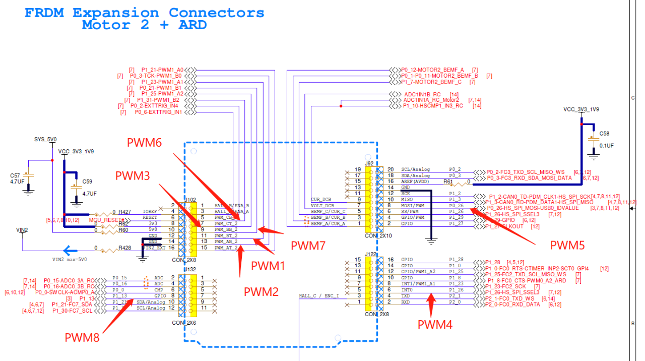
硬件连接和测试波形如下图所示,因示波器通道有限,只贴出 PWM1、PWM2、PWM3、PWM4 的波形,其他 PWM 正常产生。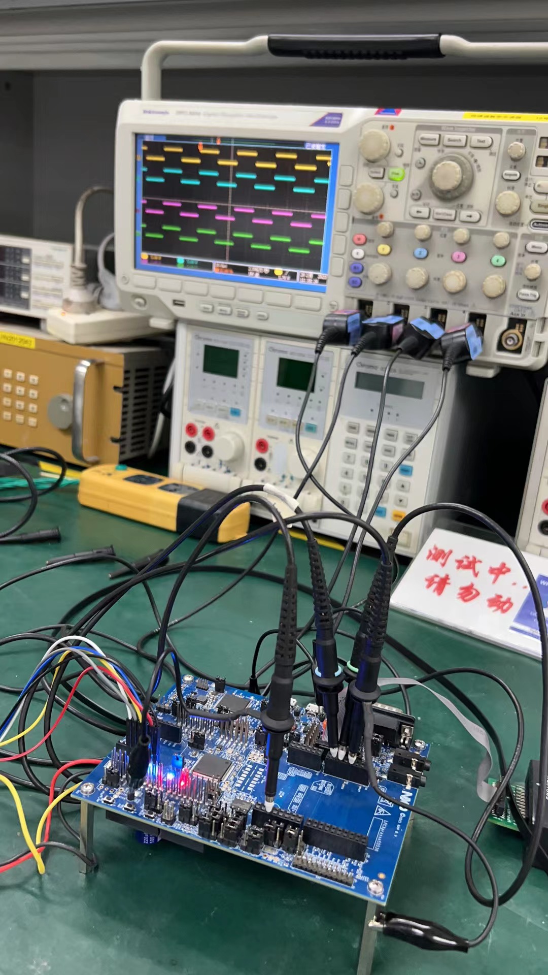
6. 参考文档
LPC5536 参考手册:
https://www.nxp.com.cn/docs/en/reference-manual/LPC553xRM.pdf
LPC55S36-EVK 开发板资料:
评论